LiPo (or so) over-discharge protection
why to protect a LiPo against over-discharge?
A LiPo cell should never be discharged bellow a specified value defined by the manufacturers. This value is normally in the range of 3.0[V]/cell and 3.3[V]/cell. The Lipos are considered dangerous, and might explode during the recharging cycle. When the charge is made with an over-discharged battery, the explosion risk increases a lot. In some cases, the battery might be permanently damaged and the recharge is no longer an option. Some projects use LiPo batteries in an unattended manner, i.e. running for hours or days without constant check of the remaining battery level. Therefore, one might be interested in a solution to cut the load off before the batteries are lost.
the LT solution
The adopted circuit here was taken from an article written in 1999 by Albert Lee in Linear Technology Magazine: "4.5uA Li-Ion Battery Protection Circuit".

The main explanation about the circuit is available in the document. I present here a compendium of calculation to select the components for the circuit.
hysteresis
When the load is disconnected from the battery, it is expected that Vi increases, and the Operational Amplifier (OpAmp) switches the load ON again. With load, Vi falls down, and the OpAmp switches OFF, and so on.. This switching endless cycle might destroy your load.
A nice feature of the circuit is the hysteresis created by the presence of R5. When the battery (Vi) discharges, the commutation of the OpAmp from LOW (Load ON) to HIGH (Load OFF) happens at Vi=Vi_low. The resistor R5 shifts the reference level up, and reduces the risk of the switching cycle. Vi should reach Vi_high to have the load ON again.

basics
Note that the circuit (and the explanation in the article) compares two different voltages, one created by the divider R3/R4, and the other by R1/Vd/R2/R5.
The voltage divider is really basic. Given an input voltage, the output is proportional to the input.

The sequence R1/Vd/R2 biased by R5 gives the other reference. When the output of the OpAmp is LOW, the circuit can be modelled by this equivalent, where Vt is the difference between the LOW output of the OpAmp and ground:

When the output of the OpAmp is HIGH, the circuit might have this model, where VT is the difference between the HIGH output of the OpAmp and Vi:

formula
The voltage reference vb1 is calculated by these equations:

and vb2, by these:

objective equations
Note that the values Vi_low, Vi_high, Vd, Vt and VT are project parameters. The unknowns are R1, R2, R5 and k (voltage divider). I decided to select myself the component R2, leaving three unknowns.
With this set of three equations, one can achieve all the unknowns, given R2:

The value imin is the minimum current at the diode U2 to have a stable voltage reference. If you use the component suggested by LT, the minimum current is only 20[uA]!! I use 30[uA].
This script (python) solves the problem for a wide range of R2 possibilities, allowing the user to select easily commercial values for his own demands.
solution and test
In my case, a good starting point was a combination of R2=15[kOhm] and R5=2M2[Ohm]. All the values for the other components came nicely afterwards.
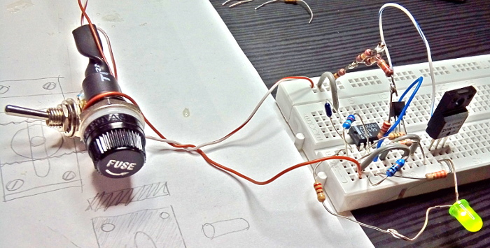
Here you have the first test with this approach:
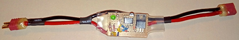
and here the final implementation of the test setup.
I hope it helps you! Enjoy!